
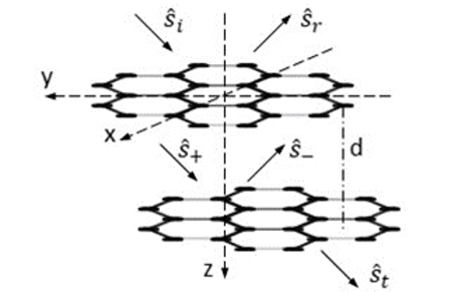
 Two-dimensional (2D) crystals are a new class of materials with a great impact on science and technology. They promise plenty of possible applications and challenges the scientists for a deep comprehension of their physical properties.We investigate the optical response of 2D crystals with the final goal of designing innovative optical coatings. In particular, their out-of-plane optical constants proved to be elusive. Recently our laboratory successfully observed them1.We are running systematic characterizations of the susceptibility and conductivity tensors of 2D crystals in the visible spectrum. We will produce a large datasheet of optical constants foreseeing new possible coatings that can be useful in many applications like sustainable constructions (for instance windows and glass facades) up to emerging technologies such as optical sensing with squeezed light.
Most relevant publications:
– He Y. et al., Weak Measurement of the Angular Goos-Hänchen Shift from a Monolayer MoS2 Immersed in a Dielectric Medium. ACS Photonics 2025.
– He Y. et al., Out-of-plane optical conductivity measured in bilayer graphene, Phys. Rev. A 2024.
– Xu Z et al., Pseudo-Brewster angles for monolayer-MoS2 and graphene immersed in a dielectric medium, Thin Solid Films, 2022.
– Xu Z et al., Optical detection of the susceptibility tensor in two-dimensional crystals, Commn. Physics., 2021.